Deep X-Ray Lithography (XRL)
Deep X-ray lithography uses synchrotron radiation to pattern thick PMMA layers (thickness: several microns up to a few millimetres) in order to achieve high aspect ratio microstructures (aspect ratio up to 100). The structures are characterised by very steep sidewalls (slope angle better than 1 mrad) and sidewall roughness in the range of 20 to 30 nm. For optical applications usually microoptical benches with cylinder lenses, prisms and fixing structures for other optical components are fabricated. The structures are either used as prototypes, as lost form for metal replication or as moulds to fabricate mould inserts.
Other application areas are several kinds of X-ray optical components like lenses and gratings. We are also involved in fabricating RF MEMS components, sensors and phantoms with high resolution test patterns.
Download technology description (PDF)
XRL will be available until end of 2024 and for proprietary (=paid) projects only.
| Name | Phone | |
|---|---|---|
| Dr. Martin Börner | +49 721 608-24437 | martin boerner ∂does-not-exist.kit edu |
Details (XRL)
Features
- Aspect ratios up to 100
- Structural height up to several millimetres
- Structural details less than 1 μm
- Slope angle better than 1 mradfor PMMA
- Slope angle about 2.7 mrad for SU-8 based resist
Limitations/constraints
- Available resists: PMMA and SU-8 based resist
- Making of prototypes requires 4 to 6 weeks process time due to prior mask fabrication (EBL needed)
Design rules
- Design required in dxf- or gds-format
- Closed polygons needed
- Rounding of structural edges (radius > 5 μm)
(exceptions for small structures possible) - Include dummy structures for stress reduction
- Homogeneous structure allocation (in case of subsequent electroplating)
Typical structures and designs

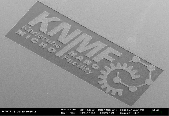
Fig. 1: Detail of an intermediate XRL mask (gold absorber height: 2.2 µm)

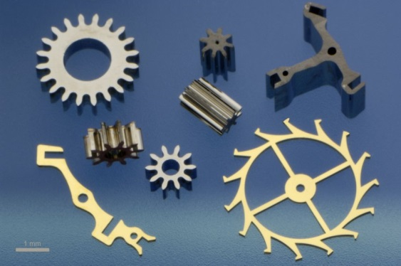
Fig. 2: Gear wheels and anchors made out of Au (99%) and Ni/Co alloy

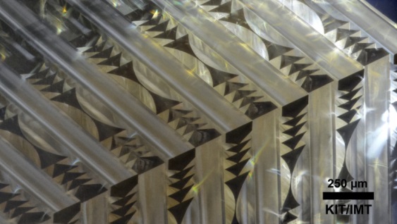
Fig. 3: Crossed Fresnel X-ray Lens with point focus (SU-8 based resist)

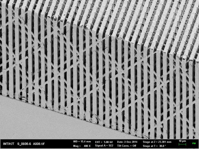
Fig. 4: High aspect ratio grating structure – increased height by “sunray” stabilization

