
Transmission Electron Microscopy (TEM)
Advanced analytical transmission electron microscopy combined with in-situ approaches
Transmission electron microscopy (TEM) enables characterization of powders and thin films (which can be prepared in a target preparation from bulk materials) by direct imaging with up to atomic resolution. The image information can be locally correlated with spectroscopic techniques (EELS/EFTEM and EDX) to provide semi-quantitative elemental composition/maps with atomic resolution. All of these techniques can also be performed in-situ, e.g. during heating, electrical biasing or straining to directly correlate structural changes and materials properties. For complex three-dimensional structures, electron tomography can be used to generate a 3D representation of the material with a spatial resolution of ~1 nm.
| Name | Phone | |
|---|---|---|
| Dr. Ali Ahmadian | +49 721 608-26531 | ali ahmadian ∂does-not-exist.kit edu |
| Di Wang | +49 721 608-28430 | di wang ∂does-not-exist.kit edu |
Details (TEM)
Equipment
-
ThermoFisher Themis-Z Double Corrected Analytical (S)TEM
-
ThermoFischer Themis 300 Probe Corrected (S)TEM
-
Philips Tecnai F20 ST
-
TEM Sample Holders:
- In-situ TEM holders
- Tomography holders
- Standard holders
Typical results
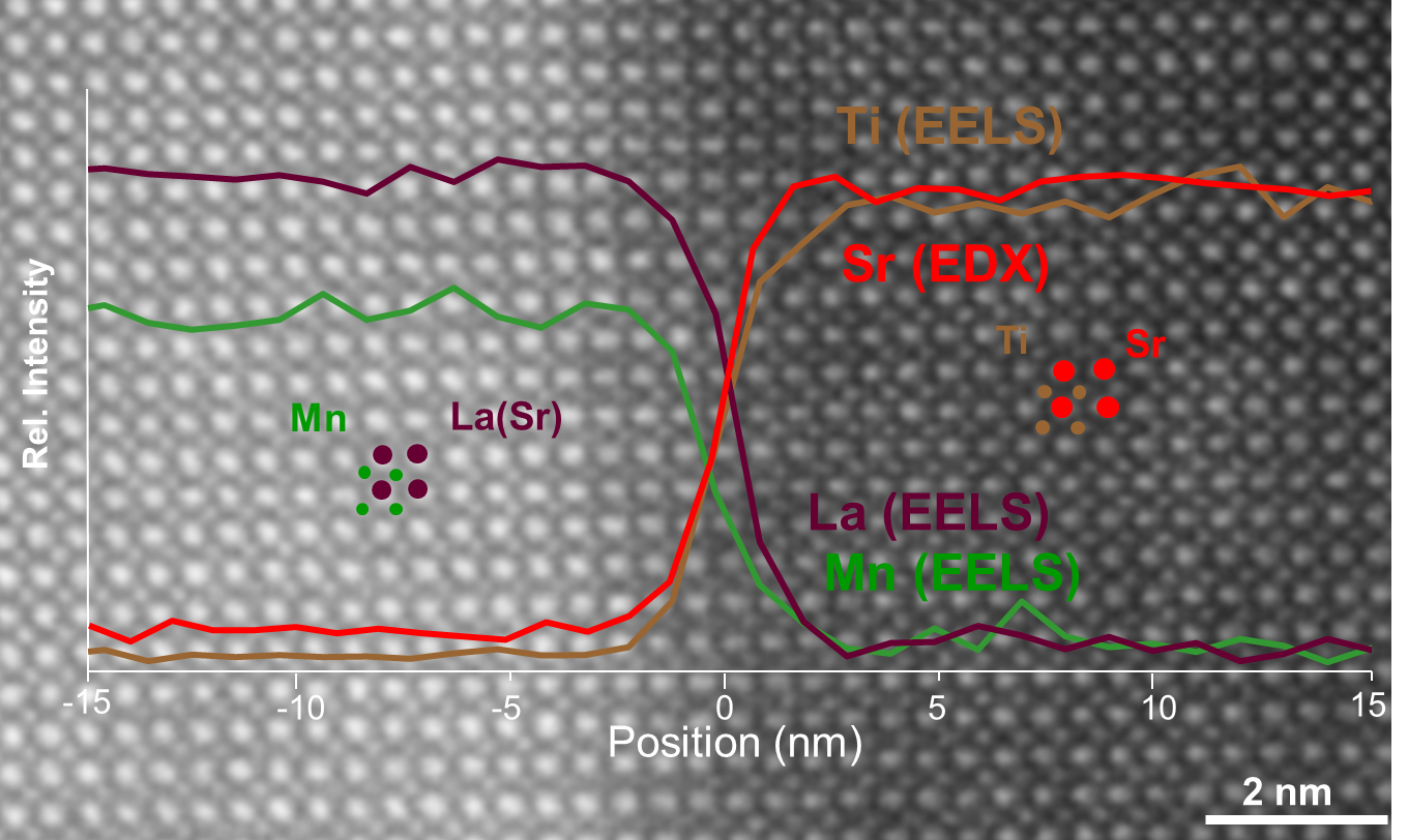
Fig. 1: HAADF-STEM image (filtered by NAD) of a La1-xSrxMnO3/SrTiO3 interface with the individual atomic columns well resolved across the interface. Overlaid is an EELS/EDX intensity profile across this interface. P.M. Leufke and D. Wang et al., Thin solid films, 2012, 520, 5521-5527.
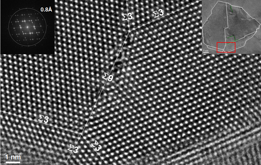
Fig. 2: Atomic resolution TEM image of a triple and a quadruple line at the interface between Σ3 boundaries and a Σ9 boundary in nanocrystalline palladium. H. Rösner and C. Kübel et al., Acta Mat., 2011, 59, 7380-7387.
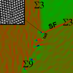
Fig. 3: Geometric phase analysis reveals the local strain distribution around the triple line in the image above. H. Rösner and C. Kübel et al., Acta Mat., 2011, 59, 7380-7387.
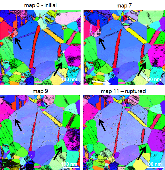
Fig. 4: In-situ orientation mapping (different color correspond to different crystal orientations) of the grain structure changes in nanocrystalline gold during straining – selected images of the straining series showing anomalous grain growth. A. Kobler and C. Kübel et al., Ultramicroscopy, 2013, 128, 68-81.
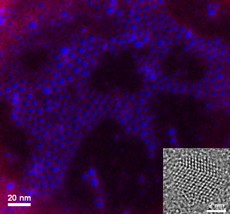
Fig. 5: EFTEM mapping (Si-blue, C-red) and HRTEM image of nanocrystalline silicon particles with a covalently bound C18 shell. The EFTEM maps reveal the ~1.2 nm wide carbon shell around the silicon core. Sample provided by G. Ozin, University of Toronto.
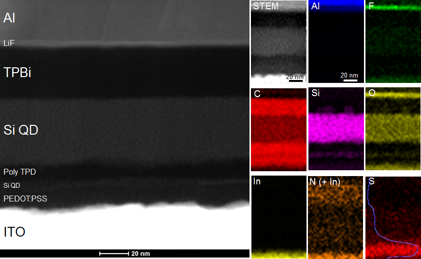
Fig. 6: HAADF-STEM image with EDX compositional mapping of the different layers in a silicon quantum dot based organic LED (SiLED). F. Maier-Flaig and C. Kübel et al., Nano Letters, 2013, online; DOI: 10.1021/nl400975u.
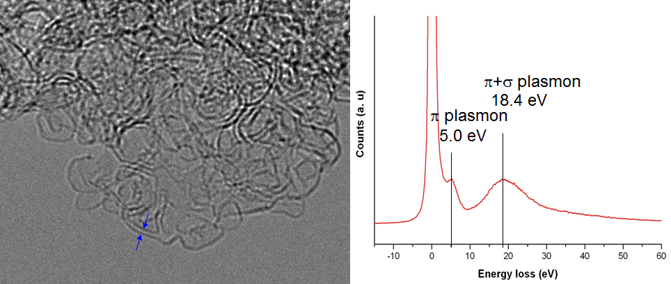
Fig. 7: HRTEM image of nano graphene with the corresponding low-loss EELS spectrum showing the characteristic π and π+σ plasmon losses. J. Biener and D. Wang et al., Adv. Mater. 2012, 24, 5083–5087.
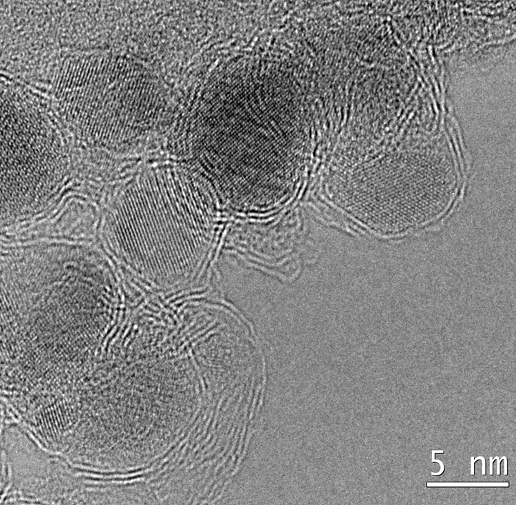
Fig. 8: HRTEM image of a Fe/LiF/C anode for lithium ion batteries revealing α-iron nanoparticles each surrounded by a few graphene layers. R. Prakash and C. Kübel et al., J. Power Sources, 2011, 196, 5936-5944.
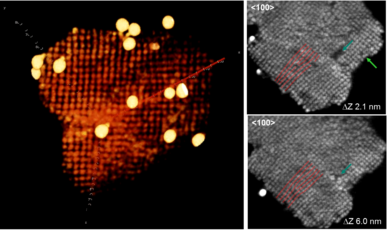
Fig. 9: Electron tomographic reconstruction of a self-assembled CdS nano cluster superlattice (with additional 5 nm gold particles in yellow). The two digital slices, one unit cell apart, show a single vacancy, an extended vacancy and dislocations in 3D. T. Levchenko and C. Kübel et al., Chem. Eur. J., 2011, 17, 14394-14398.
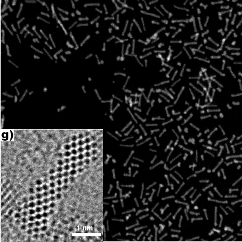
Fig. 10: HAADF-STEM and HRTEM imaging of uniform ThO2 nanorods. D. Hudry and E. Courtois et al., Chem. Eur. J, 2013, 19(17), 5297–5305.