
Focused Ion Beam (FIB)
Advanced SEM anaylsis, FIB slice&view and TEM sample preparation
The FEI Strata 400S and the Zeiss Auriga 60 Dual Beam FIB are both a combination of a scanning electron microscope (SEM) and a focused ion beam (FIB) system, which allows imaging and structuring of materials at the nanoscale. The focused gallium ion beam can either be used for ion imaging or to cut predefined patterns or images in the surface of a solid. At the same time, the SEM can be used to image the nanostructures generated by FIB. In addition, it is possible to locally deposit C, Pt or W from precursor gases using the electron or ion beam. Additionally, Insulator Enhanced Etching (IEE) using XeF2 is available.
Details (FIB)
Equipment
- Tescan Solaris X Plasma FIB-SEM platform
- Zeiss Auriga 60 DualBeam FIB with EDX, EBSD and vacuum transfer system
-
FEI Strata 400 DualBeam FIB with EDX
Typical structures and designs
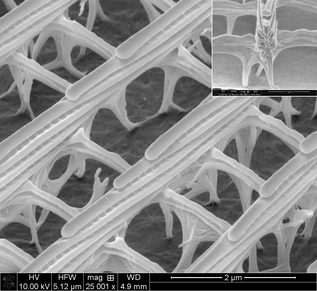
Fig. 1: SEM image of the photonic structures on a butterfly wing with a FIB prepared cross-section in the inset.
In collaboration with R. Siddique and R. Prang, KIT.
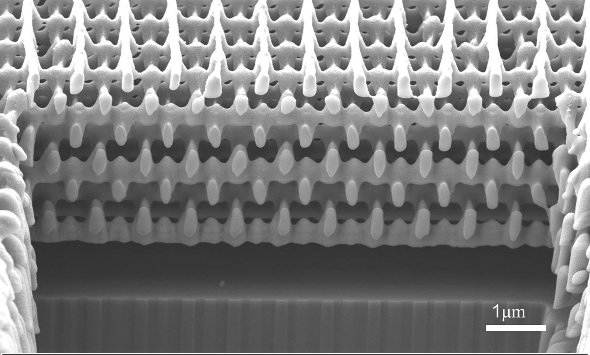
Fig. 2: Cross-sectional analysis of a photonic crystal generated by 3D direct laser writing.
In collaboration with NanoScribe and T. Scherer, KIT.
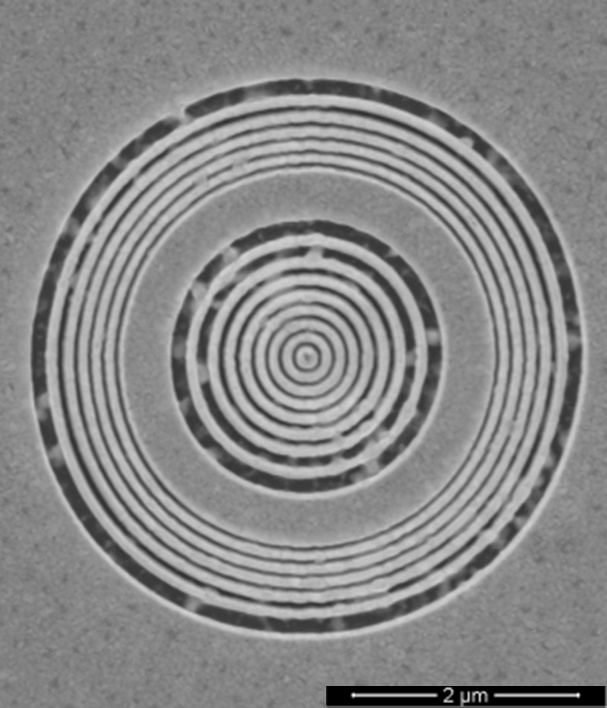
Fig. 3: FIB generated photonic structure in a thin gold film.
In collaboration with Y. Yu, IMTEK and D. Chaissing, KIT.
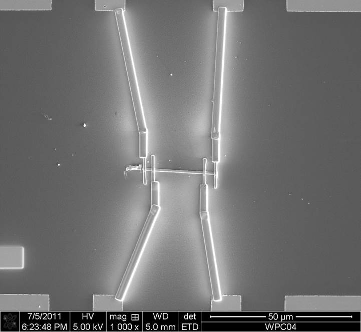
Fig. 4: Electric contacting of a silver nanowire for 4 point conductivity measurements.
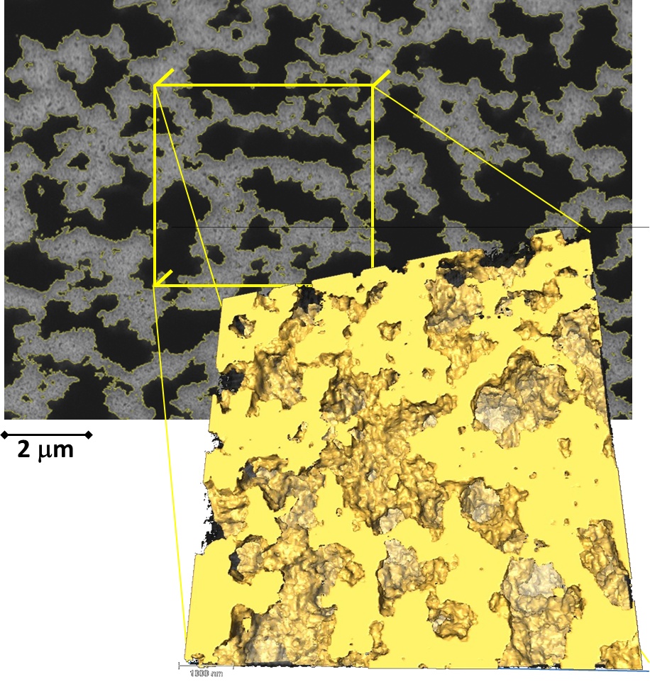
Fig. 5: 3D nanoscale morphology analysis of micro- and macroporous silica for application in HPLC: segmented digital slices through the 3D volume and volume rendering of a small area.
In collaboration with D. Stöckel, B. Smarsley, Univ. Gießen and C. Kübel, R. Prang, KIT.
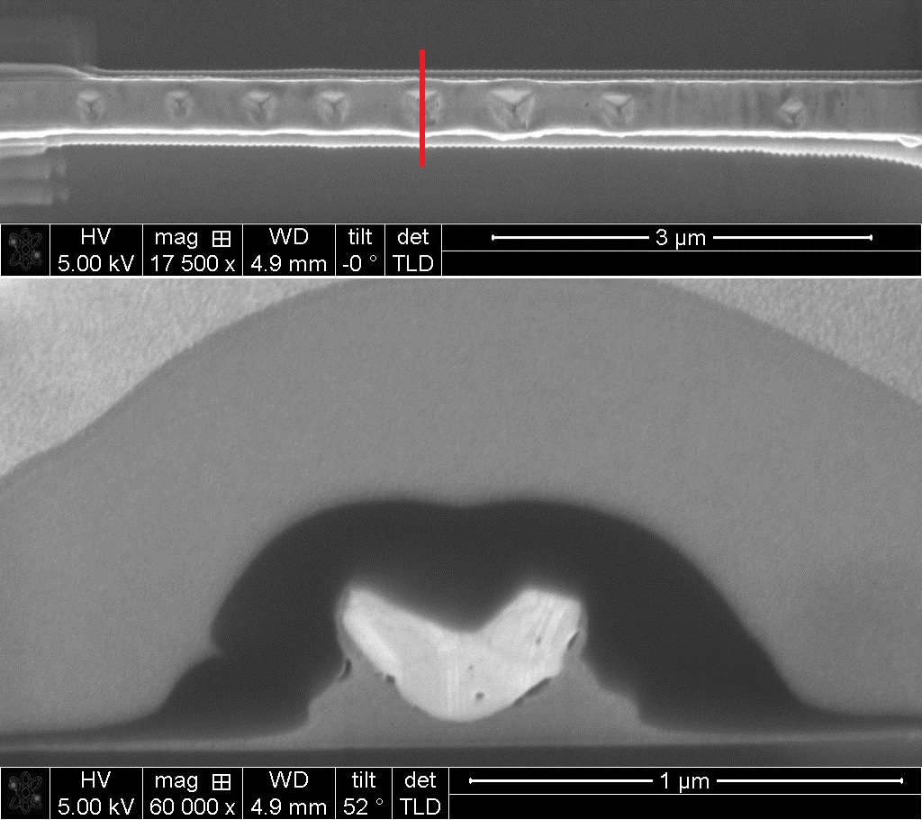
Fig. 6: TEM cross-section target preparation of a nanoindent in an Ag nanowire.
In collaboration with A. Kobler, T. Beuth and R. Prang, KIT.