
3D Atom Probe Tomography (APT)
Atom Probe Tomography (APT) allows three-dimensional imaging of a tip-shaped specimen, on which it can determine the chemical composition on the atomic scale. Typical APT specimens are sharp needles with apex diameters of about 100 nm or less. To this tip a high voltage is applied so that the surface atoms experience a field that is almost high enough to evaporate them from the surface. An additionally applied high-frequency voltage or laser pulse leads to evaporation of single ions, which are then detected on a 2D detector. This time-resolved and position-sensitive detector analyses the type of the evaporated ions by time-of-flight mass spectroscopy. To avoid lateral movement of tip atoms, the tip has to be cooled down to cryogenic temperatures. Combining the detector information, the specimen can be reconstructed three-dimensionally with almost atomic resolution. Fields of applications include e.g. metals and semiconductors.
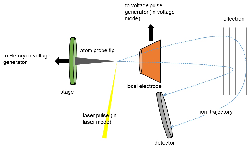
Sketch of LEAP working principle
| Name | Phone | |
|---|---|---|
| Dr. Daniel Schliephake | +49 721 608-46555 | daniel schliephake ∂does-not-exist.kit edu |
Details (APT)
Features
Voltage Atom Probe
- High Voltage: up to 14 kV
- Pulse frequency: up to 200 kHz
Laser Atom Probe
- Laser Wavelength: 343 nm, 355 nm, 532 nm, 1064 nm
- Spot size: < 3 µm
- Pulse frequency: up to 250 kHz
Field Ion Microscopy
- Imaging with He or Ne
Available preparation techniques
- Focused Ion Beam (FIB)
- Electro Polishing (only conductive materials)
Equipment
Local Electrode Atom Probe (LEAP 4000X HR)
- UV-laser or voltage pulsing
- Reflectron for enhanced mass resolution
Laser Assisted Wide Angle Tomographic Atom Probe (LAWATAP)
- 3 laser wavelengths or voltage pulsing
- Field ion microscopy mode available
Limitations/constraints
- Sample needs to be submitted in a SEM compatible sample size for FIB preparation
- Organic materials are challenging and can only be accepted in special cases
- The sample will be prepared as a sharp needle with a diameter of 20 nm to 300 nm
Materials
- Metallic Alloys, Oxides, Semiconductors
Typical structures and designs
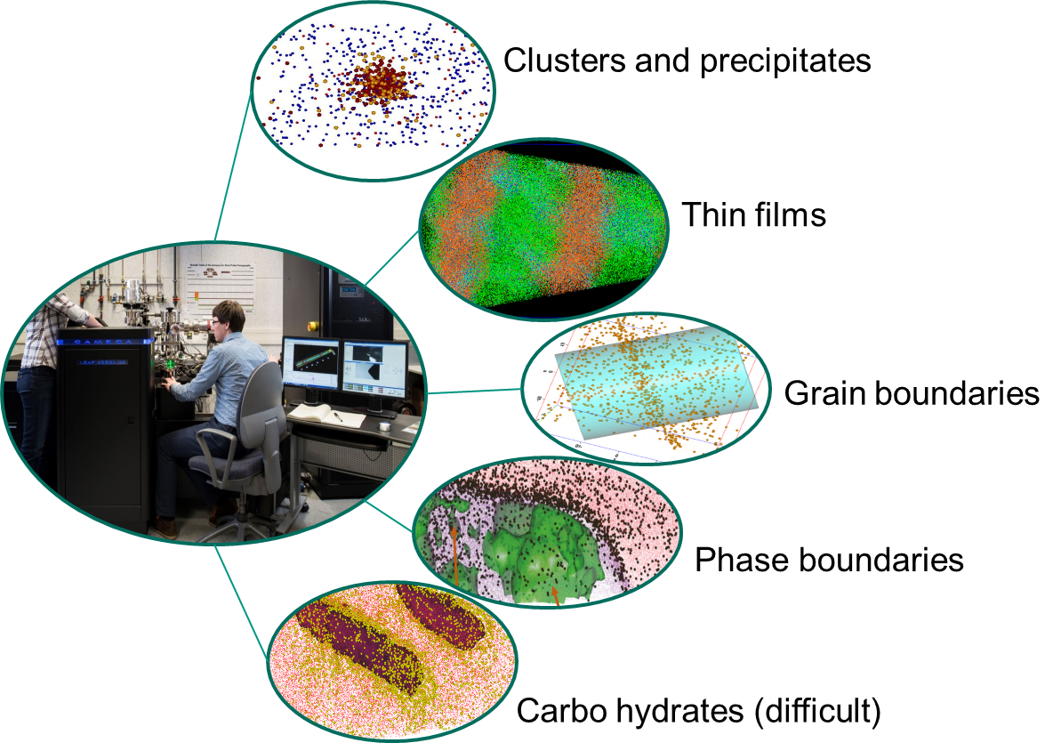
A selection of topics investigated at KNMF during the last years. The picture shows the LEAP 4000 X HR. Dots represent individual atoms.
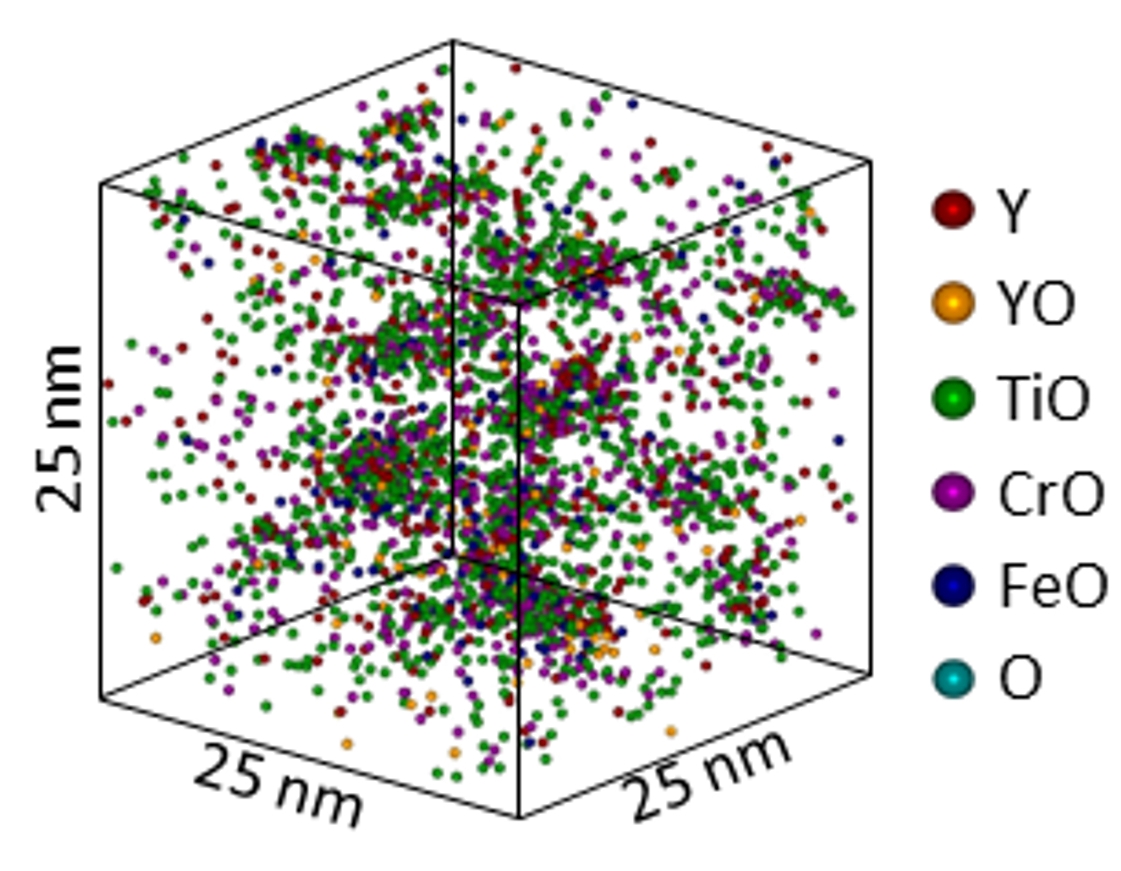
Y-Ti-Cr-O-rich clusters in an austenitic oxide disperstion strengthened ODS steel. The matrix atoms are not displayed.