
Dry Etching Cluster (DRIE)
Our Dry Etching Cluster consists of the Oxford RIE Plasmalab System 100 with ICP 380 source and the Oxford RIBE Ionfab 300. (RIE: Reactive Ion Etching, ICP: Inductively Coupled Plasma, RIBE: Reactive Ion Beam Etching). The Dry Etching Cluster is an advanced tool for micro- and nanomachining of various materials. The basic feature is a high frequency generator (RF) working at 13.56 Mhz, combined with a high vacuum chamber for wafers with a diameter of 4”. The power varies in the range of 1-2500 W. Available process gases are SF6 and O2 for silicon etching; Cl2, He, Ar and O2 for chromium and other metals.
| Name | Phone | |
|---|---|---|
| mechanical engineer Alban Muslija | +49 721 608-23011 | alban muslija ∂does-not-exist.kit edu |
| Prof. Dr. Manfred Kohl |
Details (DRIE)
Features
- Silicon etching via the cryo process (process temperatures are between -80 and -150 °C)
- Production of highly vertical, highly parallel and smooth sidewalls
- Critical lateral dimensions down to the range of 100 nm
- Aspect ratios (ARs) up to 6 are possible.
- Laser end point detection
- Metal etching via RIBE
Limitations/constraints
Silicon:
- Min. lateral dimensions: 100 nm
- Min. depth: 50 nm
- Max. aspect ratio at critical dimensions: 4
- Total max. depth: 40 µm
Chromium:
- Min. dimensions in lateral: 100 nm
- Selectivity over resist: 1:1
- Etch rate: 25…35 nm/min
Materials
- Mask material: PMMA, SiO2, ma-N 2401
- Structures on Si fragments or complete 4” Si wafers
Notice: Only silicon and chromium substrates can be processed reproducibly with standard processes at the moment.
Design rules
- Explicit and unambiguous layout according to the mentioned limitations.
- Markers for the better localization of the structures, e.g. in the SEM
- If the micro/nano structure is already written onto the substrate, the mask material has to be PMMA, SiO2 or ma-N 2401
- If combined with the KNMF e-beam, specific limitations concerning the e-beam design rules have to be considered
Typical structures and designs
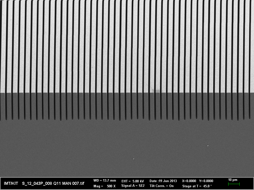
Fig. 1: Deep etched silicon gratings
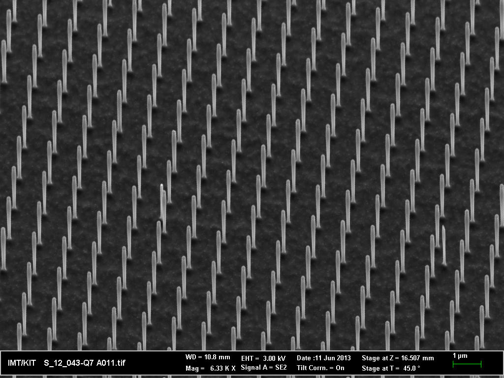
Fig. 2: Silicon nanopillars with high aspect ratio
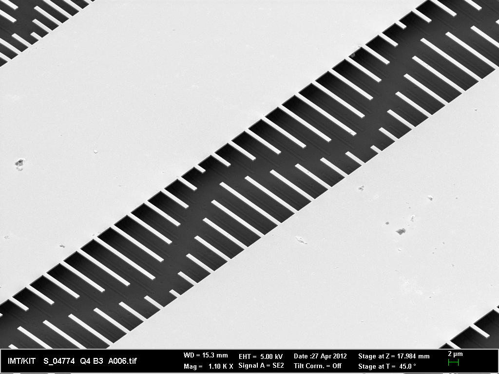
Fig. 3: Freestanding cantilevers in silicon
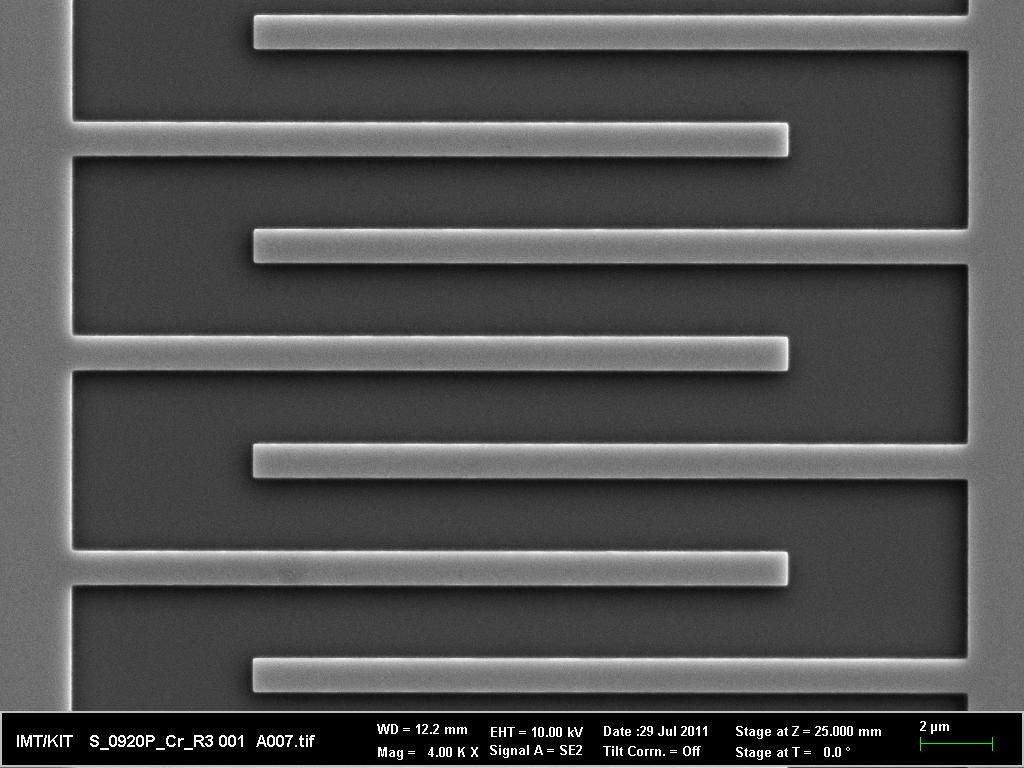
Fig. 4: Cantilever structures in chromium