
Atomic Force Microscopy (AFM) and Optical Nano-Metrology
Atomic Force Microscopy
Since its invention in 1986, the atomic force microscope (AFM) has become widely used for inspecting sample surfaces down to the atomic scale. The experimental setup of an AFM is based on a simple concept: it detects forces acting between a sample surface and a sharp tip mounted on a soft leaf spring, known as a cantilever. A feedback system controls the vertical (z) position of the tip on the sample surface, maintaining a constant deflection of the cantilever (and thus a constant force between the tip and the sample). By moving the tip relative to the sample in the x–y plane using piezoelectric drives, the actual z-position of the tip is recorded as a function of the lateral x–y position with high precision. The resulting data represent a map of equal forces, which can be interpreted as the surface topography. The lateral resolution (x–y) depends on the tip radius, which ranges from 10 to 20 nm, while the vertical resolution (z) is typically better than 1 nm. For specific cantilevers, the lateral resolution can be less than 1 nm, depending on the tip radius and geometry.
Optical Nano-Metrology (Contact: Richard Thelen)
Compared to using only AFM, we expand the application range with two optical metrology devices: a confocal scanning microscope and a vertical scanning interferometer. The confocal scanning microscope is best suited for surfaces with high texture, such as paper, crystalline, or porous surfaces. In contrast, the vertical scanning interferometer is ideal for smooth and thin layers or large areas with low z dimensions. While the lateral resolution of both optical metrology systems is limited to about 250 nm, the z resolution is approximately 2 nm for the confocal system and exceeds 0.5 nm for the vertical scanning interferometer when using phase shift imaging. These optical measurements are very fast.
Both instruments support AFM measurements by providing valuable information about sample properties, helping to determine whether it makes sense to apply AFM. AFM is the ultimate 3D metrology technology but is applicable only if the sample meets high demands on flatness, roughness, and cleanliness. We can easily check these requirements with the optical instruments located in the same clean room.
Details (AFM)
Features
- Measurements in different modes and techniques
– Contact mode
– Dynamic modes (tapping, AM-mode, ...)
– Friction force microscopy (FFM)
– Magnetic force microscopy (MFM)
– Electrostatic force microscopy (EFM)
– Kelvon probe force microscopy (KPFM)
– Nanolithography option
– Nanoindentation option - Large sample sizes (up to 8’’ wafer)
- Large scan ranges (up to 800 μm x 800 μm)
- Measurement in ambient conditions and fluids
- Combination of AFM and optical microscopy
- With motorized stages installed, the instruments can perform correlated measurements
- Sample heating and cooling during scanning (-30°C up to 200°C)
Limitations/constraints
- Sample should be smooth and flat
- Maximal sample height is restricted to 2 cm
Typical structures and designs
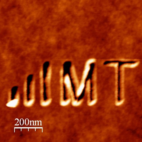
Fig. 1: Nanolithography on a PMMA substrate
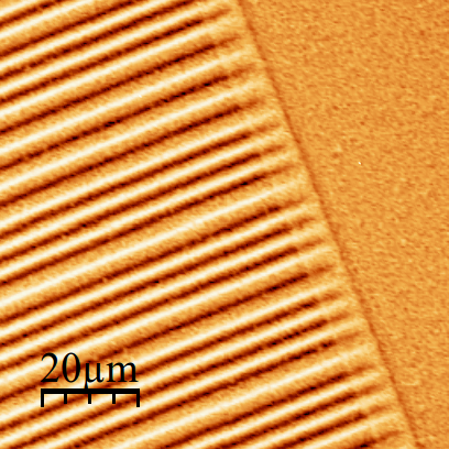
Fig. 2: Magnetic signal measured on a 1.44 MB floppy disk
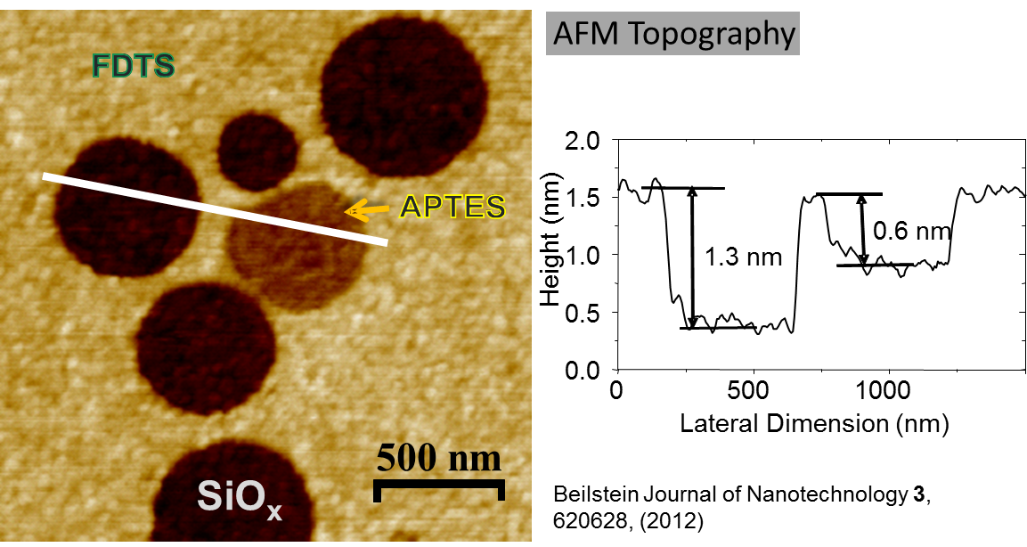
Fig. 3: Topography of a Teflon-like self-assembled monolayer (FDTS) on Silicon. Pores with 1,3 nm depth were prepared by Polymer Blend Lithography (PBL). One pore is filled with a 0.7 nm thick amino-functionalized monolayer.

Fig. 4: AFM measurement: Paper fibers wetted with pencil ink
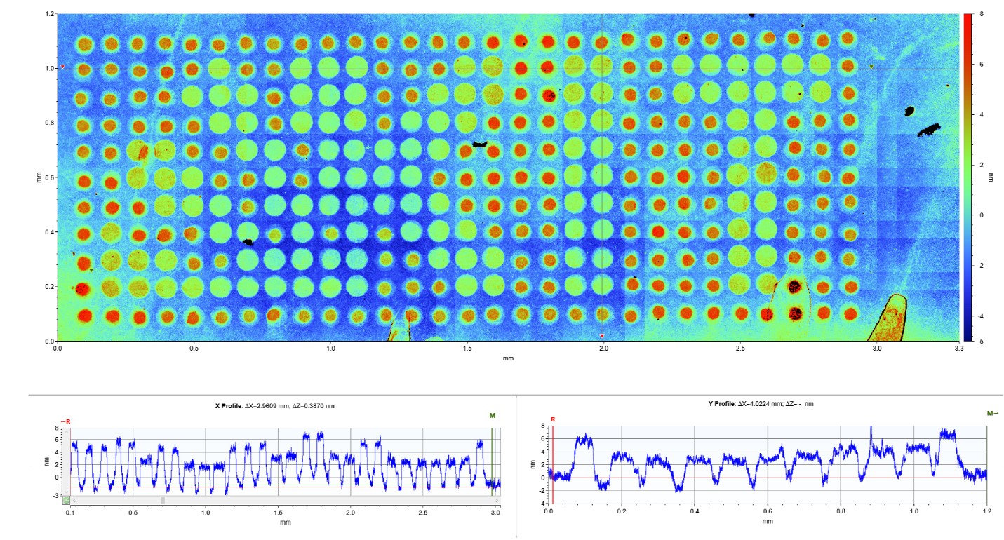
Fig. 5: Vertical Scanning Interferometer: two layered peptide spots with height of 2 nm or 4 nm only, stitched from 12x36 single frames
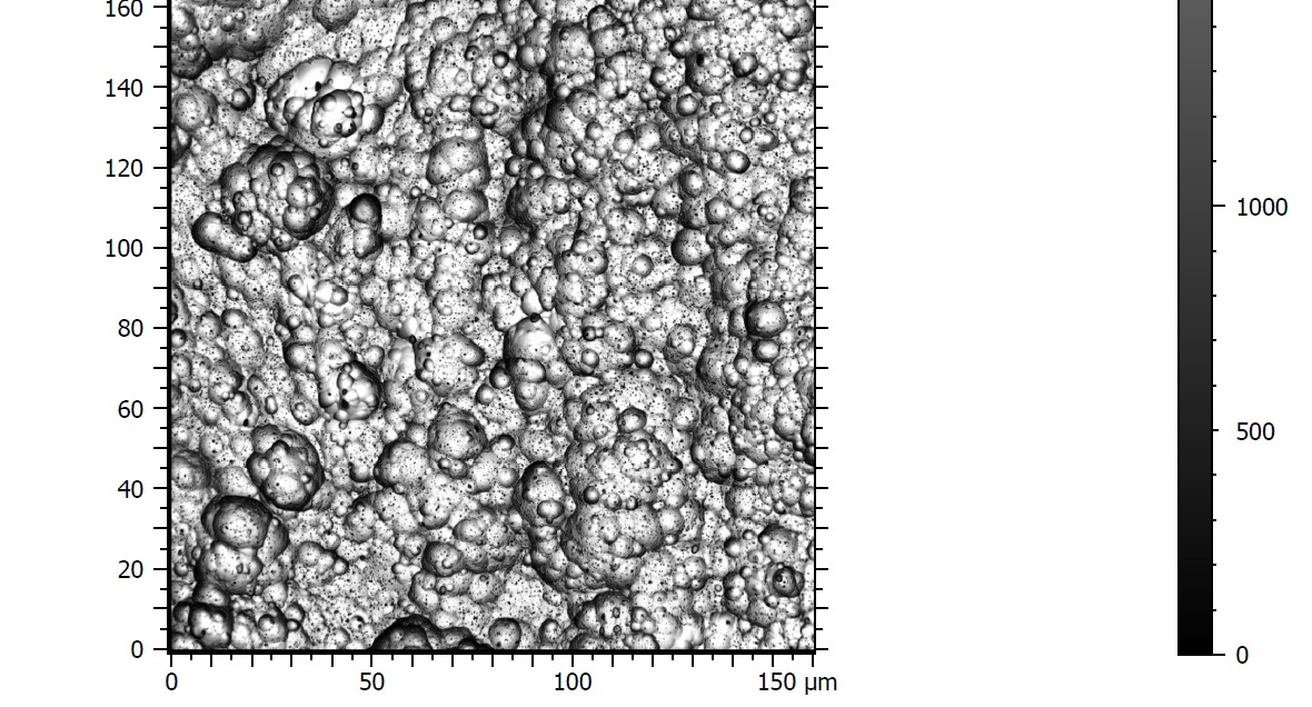
Fig. 6: Confocal Scanning Microscope: Metal surface
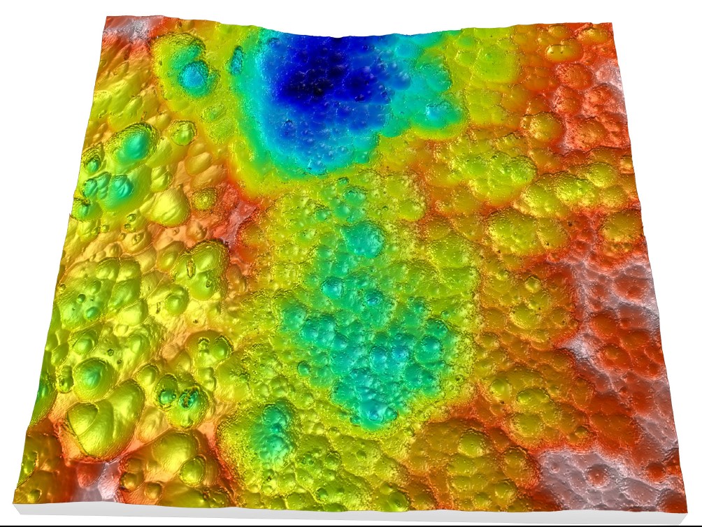
Fig. 7: Confocal Scanning Microscope: Height information gained from metal surface