
3D Direct Laser Writing (3D-DLW)
KNMFi Laboratory for Micro- and Nanostructuring
3D Direct Laser Writing is a tool to fabricate 3D freeform structures down sub µm. It is based on Two-Photon Lithography but beyond that 2D and 2.5D structures with nano dimensions are also possible. This system uses a nonlinear two-photon absorption process to modify, e.g. polymerize, a photosensitive medium at a specific point in the resist. By scanning the photoresist with a stage over this point a 3D-structure with dimensions in the submicron scale or greater can be written.
| Name | Phone | |
|---|---|---|
| Hengsbach, Stefan | +49 721 608-24441 | stefan hengsbach ∂does-not-exist.kit edu |
| Deutschbein, Celine | +49 721 608-26845 | celine deutschbein ∂does-not-exist.kit edu |
Details (3D-DLW)
Equipment
- Nanoscribe Photonic Professional GT
- Several sample holders
- Galvoscan unit
- Hybrid stage for large accurate travel distances - Critical point dryer (supercritical CO2)
- Coming soon: UV flood exposure (shell writing mode for large structures)
Features
- Resolution:
3D:200 nm lateral, 750 nm normal
2D: 180 nm - Feature Structure size: max. 600 x 600 x 3700 µm³ depending on filling factor
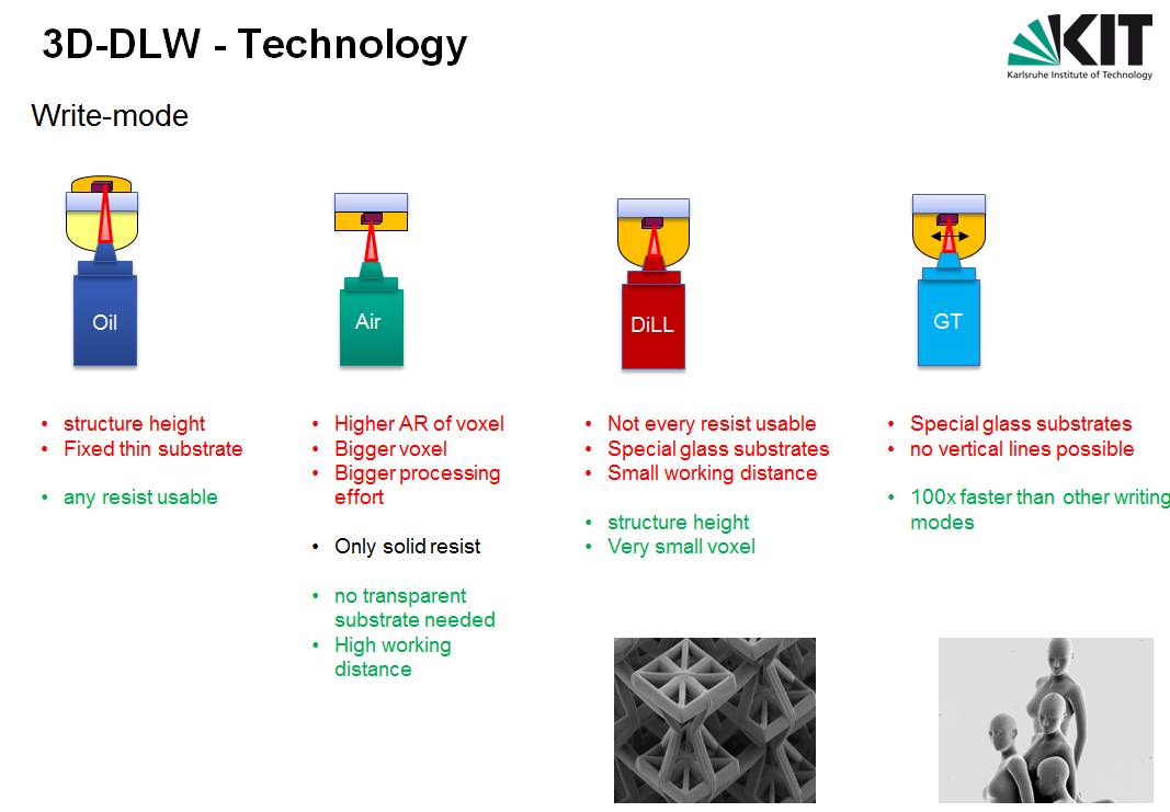
- Writing modes: piezo (100x DIP), galvoscan (63x GT, 25x GT)
- Corresponding writing fields: 300 x 300 x 300 µm³; 140 x 140 µm²; 280 x 280 µm²
- Writing times: piezo slow, galvoscan fast
- Larger areas have to be stitched
- Accessible writing area: 100 x 100 mm² where structures could be placed
Limitations/constraints
- The realizable structure size depends on the structural stability of the design
- The best results can be reached by using the IP-resists
Materials
Resists
- Negative Resists: IP-L, IP-G, IP-Dip, IP-S, and similar resists that are photosensitive at a wavelength of 380nm
- Positive Resist: AZ9260 (in preparation)
- Experimental Resists are possible, but only the Air mode objective or oil-immersion Objective are applied. Dip-in techniques can only be used with proven compatibility.
Substrates
- 25 x 25 x 0.7 mm Glass, glass covered with ITO, cover slides 22 x 22 x 0.17 mm
- Si-wafer 4’’ (100 mm)
- Si/SiO2-wafer 4’’ (100 mm
- Metallized Si-Wafer (Cr/Au)
- Other substrates have to be provided by the user.
Sample structures
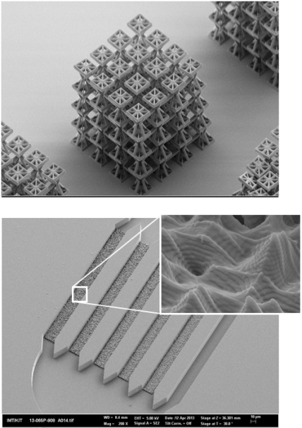 ...
...
Writing principle
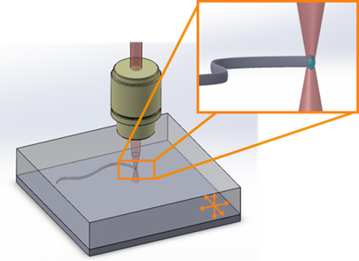
Sketch of the writing of a line in 3D-space inside a resist layer. The inset shows the modification in the voxel (blue) at the focal position. Only in the voxel two-photon absorption occurs.
Writing modes
Data
- Stl-format
- CAD data can be exported in stl-format:
- Sometimes CAD programs export erroneous stl-files. Solid works and similar programs used in mechanical engineering produce correct stl.files.
- To avoid errors within stl-files the following rules can help:
- Use correct units during contruction (µm), otherwise resolution could be bad
- Use volumes, no areas, these objects have to be closed
- Avoid Boolean operations
- Avoid duplexes (use snaps)
- Think about plane orientation. Normals are used to define interior or exterior. Therefore contruct plane consistently.
- Avoid additional structures not necessary (not written) to your part. Correction of the stl-file is nearly impossible
- In case of periodic structures a single unit cell is sufficient.