
Auger electron spectroscopy (AES)
Auger electron spectroscopy (AES) is used to determine the elemental composition and, in many cases, the chemical state of the atoms in the surface region of a solid, vacuum stable, not insulating material. AES has found widespread use in an extensive variety of materials applications, especially those requiring surface specificity and high spatial resolution. The method is based on the Auger effect which is resulting from inter- and intrastate transitions of electrons in an excited atom. Because of the relatively low kinetic energy of the Auger electrons they can only escape from the uppermost few monolayers of a specimen surface. This is the reason why this technique is such surface sensitive. In combination with Argon ion sputtering depth profiles to 1000 nm are available without prior sample preparation. In many cases there is no complex and time-consuming sample preparation needed.
| Name | Phone | |
|---|---|---|
| State certified engineer Tobias Weingärtner | +49 721 608-22913 | tobias weingaertner ∂does-not-exist.kit edu |
Details (AES)
Features
- Resolution:
– e-beam spot size at 10kV and 20nA < 24nm
– depth resolution 0.5–5nm (depending on Auger electron energy)
– energy resolution 0.5 to 0.1 % - Floating column ion gun:
– spot size 0.5 mm,
– 10 - 3000eV Ar+ ion energy
– charge neutralization possible - Semi-quantitative analysis of Li to U; quantitative analysis with standards possible
- Practical detection limit 0.5 to 5 at% (depending on elements)
- Multi-point and area analysis, line scans, element maps, depth profiles
- Coaxial electron gun and analyzer geometry
- Compucentric Zalar RotationTM for better interface resolution
- Fracture stage with liquid N2 cooling for in situ fractures (grain boundary analysis)
Limitations/constraints
- Maximum sample size Ø 60 mm
- Sample has to be solid at RT and stable under vacuum conditions (10-9Torr)
- Depending on the chemical composition samples might be sensitive to the electron beam
Equipment
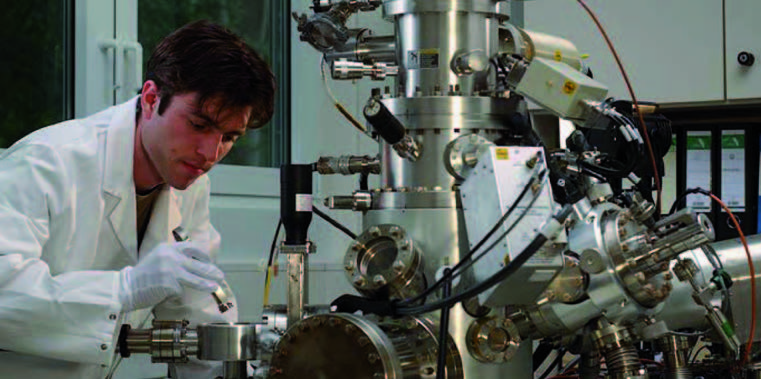
Fig. 1: PHI 680 Xi Field Emission Scanning Auger Nanoprobe
Typical measurements
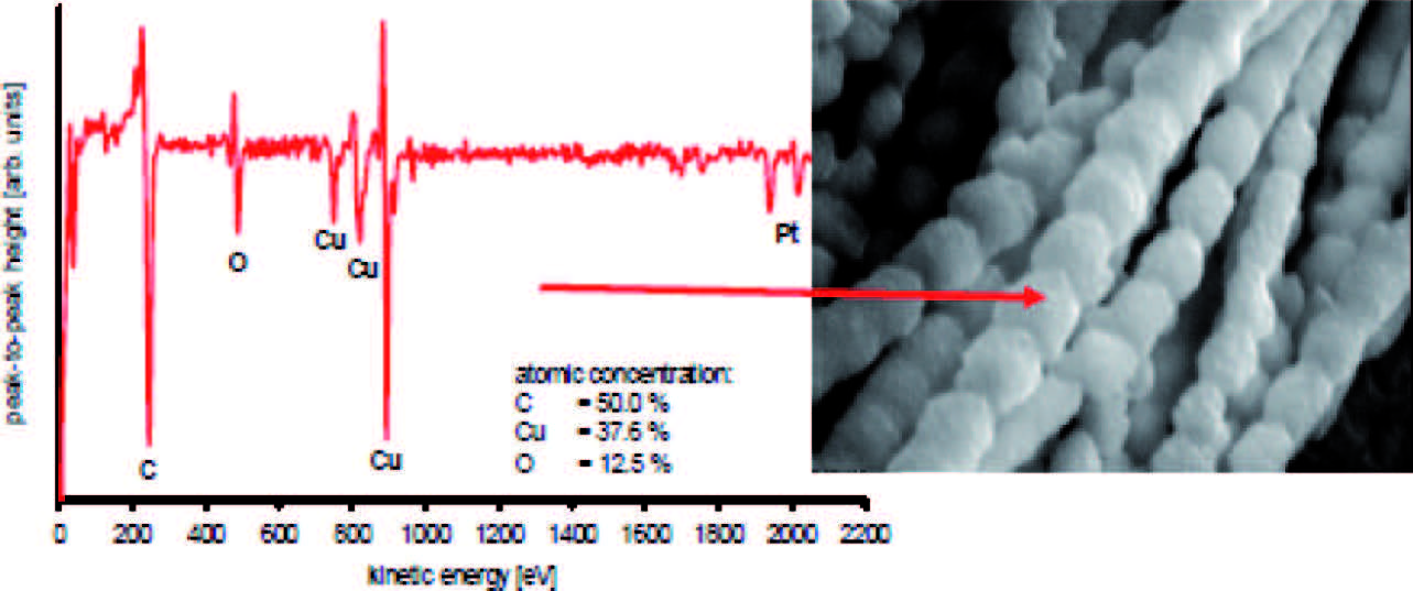
Fig. 2: Auger survey and SE image of Cu nano wires
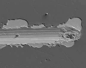
Fig. 3: SE image
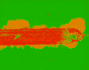
Fig. 4: AES element mapping
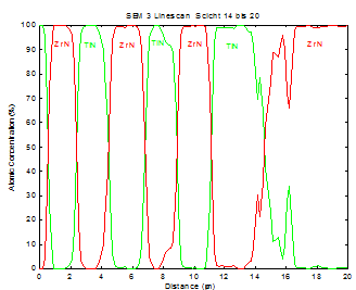
Fig. 5: AES line scan
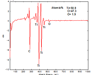
Fig. 6: AES spectrum
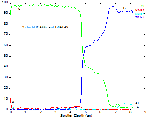
Fig. 7: AES depth profile