Direct Laser Writing (DLW)
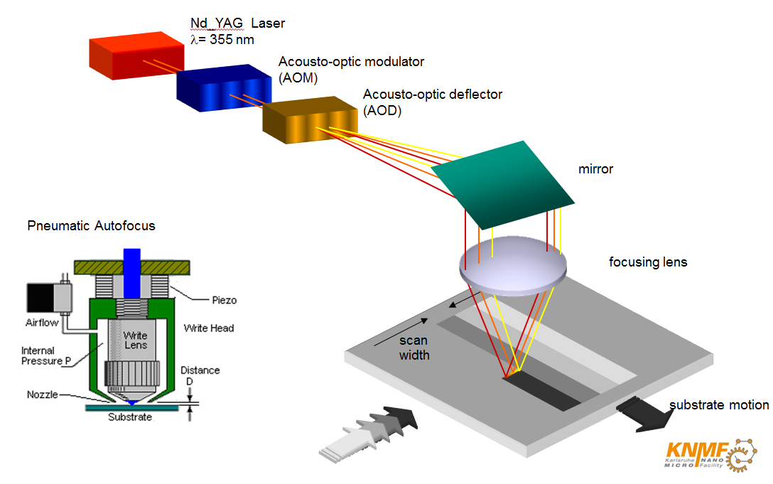 With DLW resist 2D-patterns in the µm-range are written in a photo resist layer on a substrate with a focused laser beam. No mask is needed as in conventional photo lithography.
The writehead allows feature sizes down to 2.5 µm with a substrate size up to 6”. The machine complements E-Beam lithography and is a less expensive and faster alternative for structures without nano sized features. Typically this method is applied to generate first prototypes and allows a faster iteration.
Due to the used wavelength of 355 nm it is possible to pattern thicker resist layers (e.g. SU-8 type resists). The focusing of the laser beam leads in this case to sloped sidewalls (< 5°).
In case of reflective substrates a bottom antireflection coating (BARC) has to be applied, which may be considered in the whole process layout.
| Name | Phone | |
|---|---|---|
| Stefan Hengsbach | +49 721 608-24441 | stefan hengsbach ∂does-not-exist.kit edu |
Details (DLW)
Equipment
- Heidelberg Instruments DLW66 fs
- Writehead 10 mm and 4 mm (lower and higher resolution)
Features
- No mask needed
- The wavelength of the Laser (355 nm) allows to expose SU-8-Resist up to 300µm thickness and AZ-Resists up to 7µm thickness.
- Writing speed is 35 mm²/min. A 4“ wafer will be written in round about 3 hours.
Limitations/constraints
- The structure sidewalls are not vertical in case of thicker resist layers
- Aspect ratios up to 4 are possible depending on structures and/or resists
Materials
- Resists: AZ1505, AZ4533, SU8 and similar resists
- BARC: BARLI-II
- Substrate properties:
- flat
- roughness peak to peak < 80 µm
- 100 µm < thickness < 2500 µm
Data
- Data File format: gds-II, dxf (2D), cif
- To work with good files the following hints are very useful:
- closed polylines should be used
- layers should not be named "main"
- define proper scale before designing your pattern
- use appropriate number of points in polygon approximation
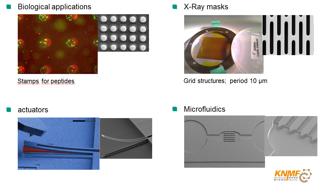
Structure examples