Helium Ion Microscope (HIM)
The Zeiss Orion NanoFab allows high-resolution imaging with high surface sensitivity and a depth-of-field 5-10 times higher than in a modern FE-SEM. The focused helium and neon ion beams can be used for machining at the nanoscale with feature sizes 10-20 times smaller than achievable using a gallium FIB. The tool is well suited to imaging challenging samples such as polymer-based systems and biological specimens without additional sample coating. For electrically insulating samples, positive charge resulting from the ion beam is compensated by using an electron flood gun directed at the sample. In addition, it is possible to locally deposit Pt, W, or SiO2 from precursor gases using the helium and neon ion beams.
Details (HIM)
Features
Zeiss Orion NanoFab with He and Ne ion beams
- Resolution: ≤ 0.35 nm
- Resolution (He/Ne) ≤ 0.5 nm / ≤ 1.9 nm
- Acceleration voltage (He/Ne) 10 kV – 35 kV / 10 kV – 30 kV
- Beam current (He/Ne) 0.1 pA – 100 pA / 0.1 pA – 50 pA
- Field of view 900 μm – 100 nm
- Detectors: Everhart-Thornley Secondary Electron Detector (ETD)
- Charge compensation: Electron flood gun
- Chamber base pressure 2 x 10⁻⁷ Torr
- Stage:
Tilt 0-56°
Maximum travel in x and y ±25 mm from center - Gas injection system for Pt, W, insulator (Siloxane)
- NanoPatterning and Visualization Engine (NPVE) for advanced patterning
Limitations/constraints
- Sample has to be a solid at room temperature, dry and stable under high vacuum conditions
- Maximum sample height 10 mm
- Samples should be very clean prior to imaging to minimize carbon contamination
Application examples


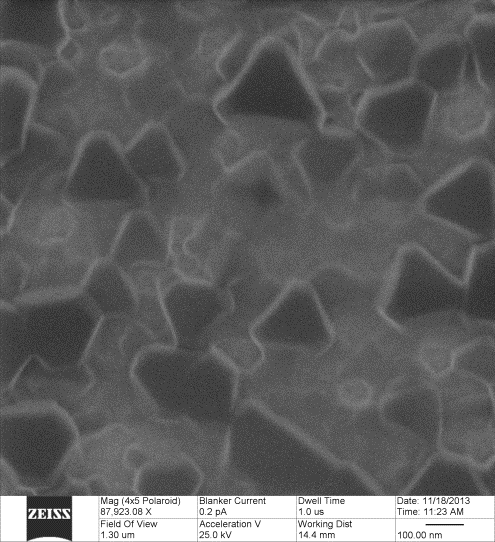
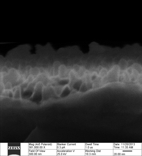
Fig. 1: 3D SURMOF (plan view and cross-sectional view, collaboration with H. Gliemann, IFG, KIT)


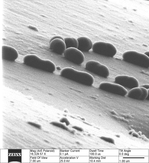
Fig. 2: Biofilms E. faecalis DSM 2570 (24 h incubation at 37°C) on Calgary Biofilm Device (CBD) (collaboration with P. Sanyal and A. Ulrich, IBG, KIT)

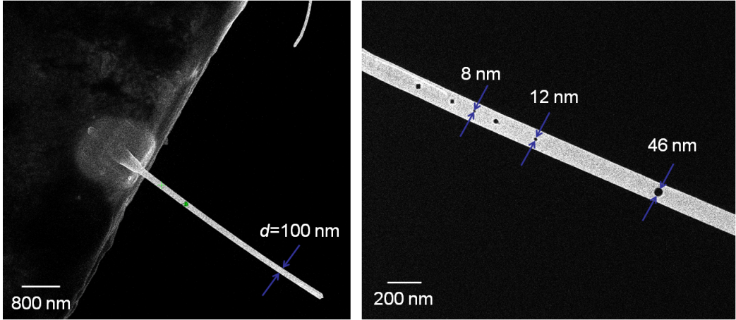
Fig. 3: Nanostructuring of Au nanowires (collaboration with O. Kraft, IAM-WBM, KIT)

